- Details
BMS Readout Deployment
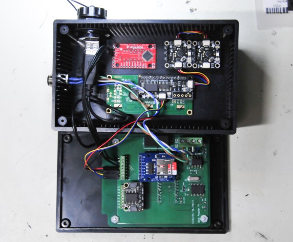
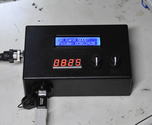
I designed an updated version of the BMS PCB, one that has connections to handle all the modules that are part of this system. During the time I waiting for the PCB to be fabricated I realized that all the Adafruit modules could be connected with the Stemma QT/Qwiic connector system. These are a connector specifically for I2C communication. Just 4 wires, ground, +5v, SDA and SCL and they come preassembled in all kinds of configurations (link). Using this system, I reduced the number of wire connections to the PCA that were required. I connected the two rotary encoders and the LCD with the Stemma QT cables. On the new PCA by using the Stemma QT connector system I only need one 4-wire connection to the PCA. The enclosure for the BMS Reader is the same Jameco enclosure I am using for some of the BMS modules (see the blog below BMS Ready for Deployment). I machined the Jameco enclosure to fit the LCD, 7-segment display and the rotary switches. You can see the enclosure, PCA and all the connections inside the enclosure in the photos below. I now have two rotary encoders because I found that was easier in code to have one to select the cells in the battery and one to select the battery module to read. The enclosure has the same 12mm 4-pin connector that I have on all the BMS modules for power and CAN BUS. I also added a USB feedthrough because although, all the battery cell measurements will be saved on the MicroSD card, I will eventually want to get all the data into my computer. With the USB feedthrough I can do that without taking the enclosure apart, which is what I would have to do if I wanted to read the MicroSD card. It would have to be removed to be read by the computer.
Add a comment
- Details
BMS Readout Prototype
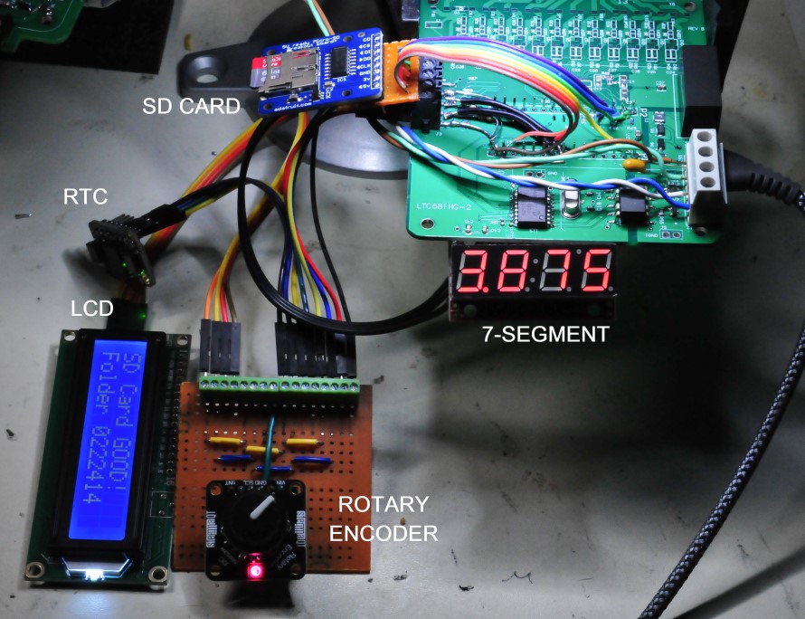
I realized after I deployed the first four of the BMS modules on my batteries that the only way I could read and record the cell voltages was with a laptop computer, which was also how I could only measure the cell voltages with the Demo BMS that I started with (see Blog below Battery Maintenance System). Now because of the CAN BUS I can read and record all four batteries and eventually all nine with just one connection. However, using a computer is not always possible and also difficult to impossible to use while driving. I decided to make a system that could readout and record all the battery cell voltages, that could be connected to the batteries and operated at any time, or provide measurement and storage while driving the car. The readout system would need a display, a storage system and a Real Time Clock (RTC) to provide a timestamp for the cell measurement. All three of those functions are easily accomplished with small, easy to program modules. A 4-digit, 7-segment LED display like I used for the instrument cluster could be used for the cell readout. For cell voltage storage a MicroSD memory card can be used. I have built several other systems with MicroSD card memory modules and they are very easy to write and read from, usually with a SPI interface. The RTC is a standard module that again I have used in many other projects. The only other component required is some type of switch system to switch the measurements from cell to cell and battery modules. I found by searching that a rotary encoder switch would be ideal for the switching system. A rotary encoder continuously provides a count of the switch position, no matter which direction is rotated. Adafruit, an on-line electronic components vendor makes a small encoder with a I2C interface called the I2C Stemma QT Rotary Encoder (link).
Since I have all of these modules, I decided to build a prototype to develop the code for the system. I will probably make a new PCB for this system because as you can see in the image below there are a lot of connections and wires that I had to add. For the prototype, I used the current design of the BMS PCA, but built one that had only the CAN BUS circuitry, the DC input and filtering and the Arduino Nano Every installed. I made a daughter board out of perfboard to provide additional connections. The modules either communicate with I2C or SPI or Serial. The Nano Every has connections for all of those communication methods. But the BMS board only has connections to the SPI buss. The 4-digit readout is perfect for displaying the cell voltage measurements as it will display to the millivolt, which is all that is needed to understand if cell voltages are changing. I have already determined the cell voltage is very repeatable and has a very small standard deviation well below one millivolt. The problem with the 4-digit is that it can only display numbers well, not letters. To get more information I decided to also add a 16 character by 2 lines LCD module. I did realize I could put the cell voltage measurement on the LCD and eliminate the 4-digit display. But I have found these kinds of LCD displays are hard to view off axis and usually cannot be seen with polarized sunglasses. The viewing angle issue is highlighted in the picture below. The 4-digit display is LED so it is viewable at any angle and with sunglasses. I will only use the LCD to display which battery the system is connected to and some information about the MicroSD card, like the folder where the data is stored. Below is an image of the BMS Readout system prototype. To record the battery cell voltages while driving I can automate the switching instead of using the encoder switch to select the cell to measure and store. The module labeled in the image below SD Card is actually a MicroSD card module that is another module offered by Adafruit (link). What is great about all of the Adafruit modules is that they always have links to code examples to drive the modules. That really makes the code development much easier. They also often have YouTube videos demonstrating the modules. Those were handy to see how the rotary encoders work.
Add a comment
- Details
BMS Ready for Deployment
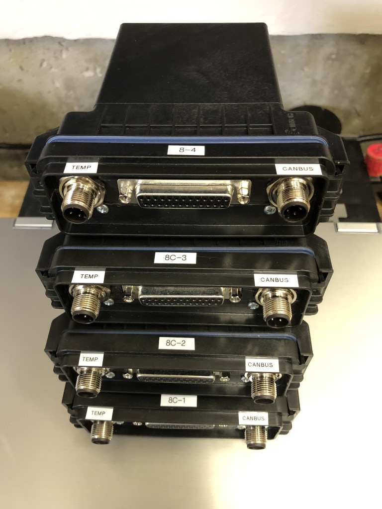
I now have four (4) BMS units built up and tested and ready for deployment I machined the front panels for the CINCH enclosures to fit the DB25 and M12 round connectors. Below is an image of the four units. I still need to make up more M12 cable sets, to connect all four units together in the car. I have the shielded cable, just need to get more M12 connectors. Just like any electronic component the connectors go out of stock at Digi key and then I have to find an alternative source. I also have to make up DB25 cables to connect the BMS units to the batteries. All batteries have the DB25 connector that was used to connect the DC2260A BMS demo board to measure the cell voltages, one battery at a time. Now the cell voltages of at least the first four batteries can be monitored together, at the same time. The BMS units will be mounted on the side of the battery box and none of the battery DB25 cables can reach that, so new cables need to be fabricated. I think connecting to the existing DB25 cables would be better for testing than creating a cable that goes between the BMS and the BMS connections on each battery.
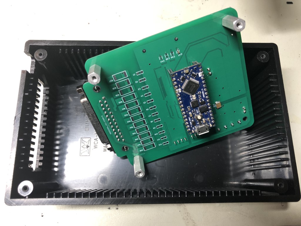
I have to use a different enclosure for the first BMS PCAs that I built up. At that time, I was not sure the Arduino Nano Every processor board should be directly soldered to the BMS PCA. The Nano is connected via SIP connectors on the bottom side of the PCA, so that it can be removed, if necessary. I have three PCAs that were assembled that way. That extra 3/8" of height means the PCA cannot fit in the CINCH enclosure. I will be using a plastic enclosure made by Jameco. See the image below. You can see the SIP connectors on the bottom side and see how much that offsets the Nano from the PCA. The PCA has standoffs in the corners to raise the board to the correct height for the DB25 connector. You can see in the image how the front of the enclosure is machined to fit the DB25. The side of enclosure, opposite the DB25 side will have the circular M12 connectors (not yet machined). These BMS units will be connected to the batteries under the rear seat, so they will be inside the passenger compartment. The Jameco enclosure does come with a gasket for the lid. Not as moisture tight as the CINCH enclosure but should be good enough inside the car.
Add a comment
- Details
Bolt Batteries Update
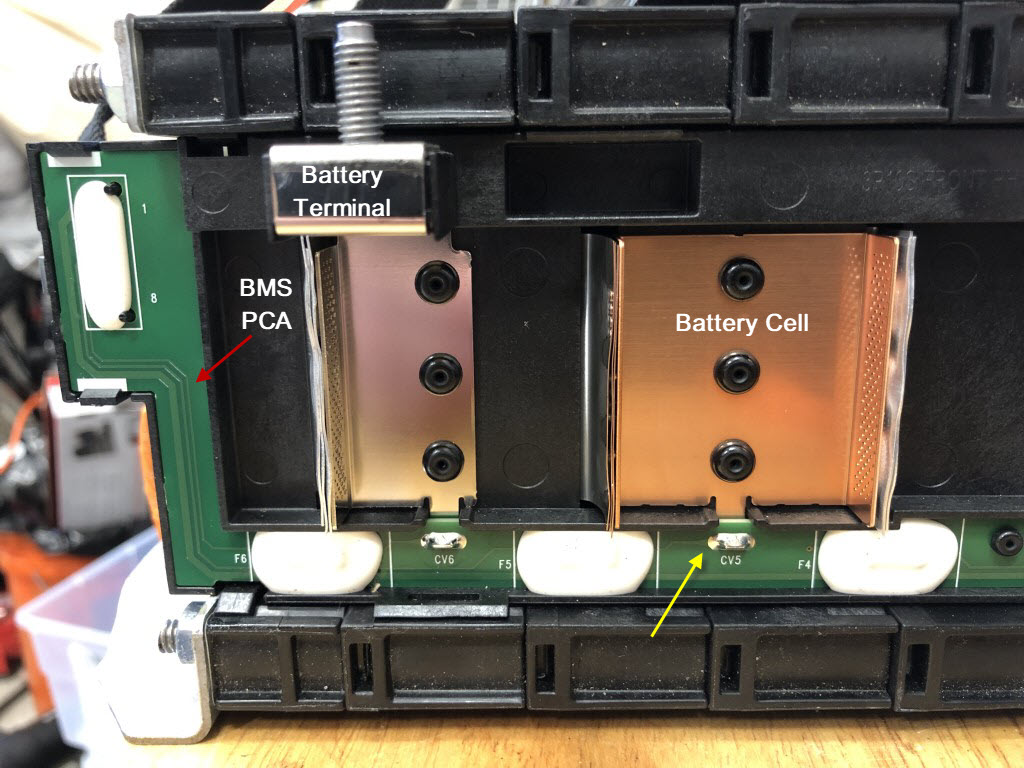
I have a video I have mostly put together but have not posted, on an issue I found with the Chevy Bolt batteries. I found it when using the Analog Devices DC2260A demo BMS board to understand more about the Bolt batteries (see Blog Chevy Bolt Batteries). Once I understood how to connect the demo BMS to the battery modules I used it to test all 9 battery modules that I had purchased. All 90 cells in the batteries were nearly the same voltage, +/- 2.5mV, but I found one battery that seemed like one of the cells was not connected. The BMS demo software showed two issues. First one of the cells would read lower voltage, second, the adjacent cell would read a higher voltage than any of the other cells. This difference was highlighted when the discharge circuit was activated in the BMS. The lower voltage cell would read nearly zero volts and the adjacent cell would read 5.46V which is clearly not possible. I believed that is just an issue with the A/D converter circuit in the BMS Integrated Circuit on the demo board and it is not reading that voltage on the cell. Analog Devices tech support said it was due to the Transistor (MOSFET) in the balancing circuit turning on full because of an open circuit. After some investigation I discovered that two connections to the battery cells were open, i.e., disconnected. On the Chevy Bolt battery module all the cells are connected to the BMS connectors on the front of the battery by two narrow PCAs that run the length of each side of the battery module (see image below). I believe what has happened is that traces on the PCAs are broken somewhere causing the open circuits. It might be where the cell is soldered to the PCA (yellow arrow in image below) although there is no visible indication of an open circuit anywhere. I solved the measurement problem by soldering wires directly to the cell solder points and bringing the wires out to the DB25 connector. What is disturbing is that this particular battery was never installed in the car. I needed to have the front battery box in my car modified to fit the 9th battery module, so I had that battery on the bench, ever since the time I received it. It was essentially delivered with that open circuit. This was discovered in December of 2020, shortly after I had received the batteries and got the demo BMS connected to the batteries. Eight of the Chevy Bolt batteries have been in the car since then and been subjected to many charge/discharge cycles, while driving the car for the past 3 years. I had used the Chevy Bolt wiring harness to make connections to all the batteries (again see Blog Chevy Bolt Batteries) so that I could connect the demo BMS to every battery and measure the cells, one battery module at a time. That is why I decided to make my own BMS, so that a BMS circuit could be connected to each battery module all the time and allow constant monitoring. Since I have been monitoring all the battery cells, I have found that 6 out of the 9 batteries received now have one or more cells that measure open, with the BMS. The other batteries developed the open cells sometime over the past 3 years, but I believe this highlights the defect that was in the LG Chem batteries that caused the battery fires seen in some of the early Chevy Bolt EVs. As a human reviewing these results, I could understand the problem with the batteries, that it is just a measurement problem. But the firmware in the Chevy Bolt BMS might not identify that problem, it there was no code to look for it. If a similar A/D converter circuit was used in the Bolt BMS and the firmware was not programmed for this problem you can image what might happen. The way a BMS typically maintains battery cells is to move charge between the cells to balance the voltage. If the BMS did not know about the open cell voltage measurement, then it might move current out of the false high voltage cell and push it into the false zero voltage cell. Over several charge cycles this could develop into real problem where the false zero voltage cell was getting overcharged and the false high voltage cell could be over discharged. Both of these scenarios could cause a battery fire because both cells would still be charged when the full pack was charged. The cell maintenance is very small amount of current but could eventually damage cells. If this was happening in over half of the battery modules in the Chevy Bolt is a wonder not more fires occurred. This is a manufacturing defect (broken PCA traces) but also a firmware issue in the BMS. The broken traces in themselves do not affect the performance of the battery module and would never lead to a fire. It is only the action of a BMS Firmware that was not programmed for this defect could cause that. LG Chem only admitted that a manufacturing defect caused the files, but said nothing about the BMS. The BMS being the cause is also the opinion of a number of automotive journalists. This issue with the open cells measurements highlights why my BMS is a Battery Monitoring System and does no cell maintenance. Three years of testing the battery modules in the car show a very narrow cell voltage distribution without doing any cell maintenance. This is an indication of how well the cells in the battery module were manufactured. It is too bad the open circuit cell voltage measurement was not identified early in the Chevy Bolt EV development. The battery fires may never have happened and the Bolt EV would still be sold by Chevy after 2023.
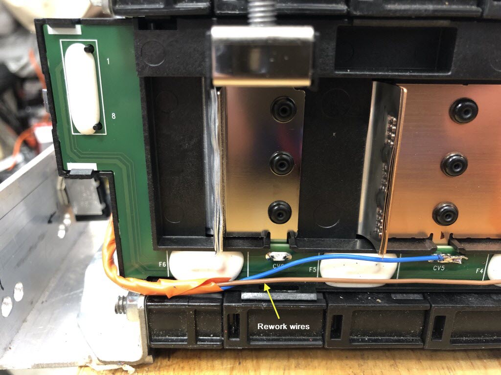
Shown below is the rework to fix the BMS circuit. The second wire goes to the 4th cell. There is another wire on the opposite side that connects to cell 5. Usually two wires are required to fix a channel in the BMS circuit.
A video of the Chevy Bolt battery is coming soon.
Add a comment- Details
BMS Deployment Testing
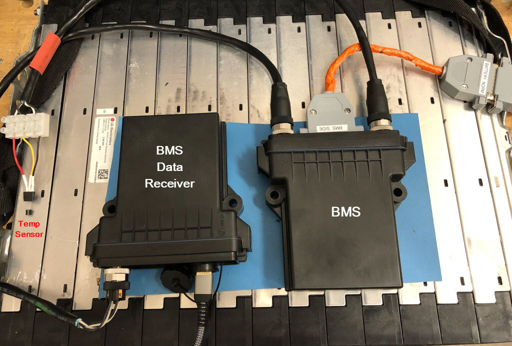
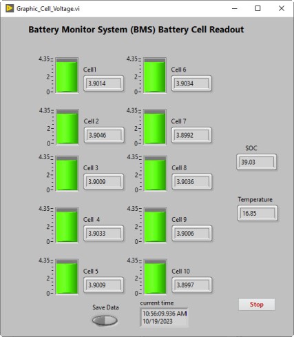
Here is the test of the BMS system before it goes in my car. The BMS assembly is in a CINCH enclosure with the M12 circular connector cables. The image below shows the testing setup with a battery module on the bench. On the left side of the image, you can see one of the one-wire temperature sensors at the end of the cable. That will be soldered to the end of the cable when deployed in the car and attached the battery heatsink surface with some conductive tape. The connections for power and CAN BUS are on a barrier strip that is just off camera to the left. The image shows the BMS with another module I put together to receive the CAN BUS data from the BMS. When deployed in the car the CAN BUS data will be handled by the processor that controls the Instrument Cluster in the dashboard. For testing and the initial deployment, I will use the Data Receiver. It is a BMS PCB with just the CAN BUS circuitry and the Arduino Nano Every installed. It is also mounted in a CINCH enclosure and has the M12 connector for the CAN BUS connection and power. The Nano Every receives the CAN BUS data by SPI from the CAN BUS circuit and then sends the data out via the serial bus, on the USB connector. I wrote a program to read the serial data and interpret the CAN BUS data, which is all in HEX. A screen shot of the application is shown below the battery test image. The application converts the HEX string into decimal values and displays that with a “fuel gauge” graphic for each battery cell. The program can datalog the data to the hard drive. The cell voltage measurement is updated every 2 seconds. The LTC6811-2 BMS IC can be read faster than that but, there is overhead in converting the voltage values to decimal to display. The application also displays the temperature measured from the one-wire probe and the state of charge (SOC). This is the total voltage of all the battery cell voltages added together and is the voltage that is measured on the main battery terminals. The values show the battery in nearly fully charged.
Add a comment